by Nat Levy
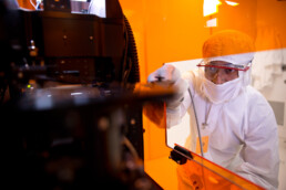
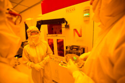
In a small lab, surrounded by fellow students, Young He equips a second layer of protective equipment. A blue plastic smock and a face shield cover his clean suit and booties.
He grabs a large plastic bottle and begins carefully pouring a liquid as the rest of the cohort stands back, an undercurrent of tension in the sterile air.
Have you seen Breaking Bad?
A fellow student asks us, breaking the silence. The acid they use in the famous bathtub scene? This can do the same thing.
That gets a chuckle and cuts the tension, but the chemical itself, hydrofluoric acid, is no laughing matter. It is corrosive to metals and tissue. All students handling it receive safety instructions and are required to wear protective gear. In the semiconductor industry, it is used for etching, the selective removal of materials and layers during manufacturing.
He, a senior electrical and computer engineering student from Houston, has the honor
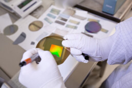
of performing this task today, but in other weeks, his classmates will do it. They’re all rotating across several stations. Some work on the etching process. Others apply photoresist, a light-sensitive material. And still others line up a mask that directs light at parts of a chip.
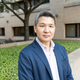
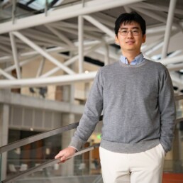
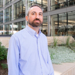
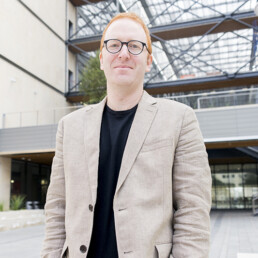
Young He, a senior electrical and computer engineering major, in a semiconductor lab.
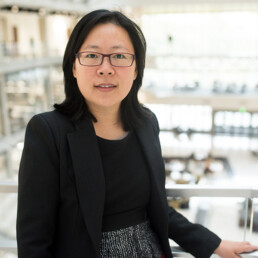
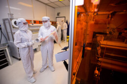
Siyu Wu, a fifth-year Ph.D. student in electrical and computer engineering, guides the students through the process. Today is their first time using the machines on their own, and she has to make sure the equipment works, the experiments stay on track and everyone follows safety and operational protocols.
After several more weeks of lectures and labs, students will hopefully create functional integrated circuits — the devices that tie together semiconductor materials, transistors, resistors and more to power large electronics — that can be tested for performance. This hands-on experience is virtually unmatched in higher education, and it helps prepare students for careers in the burgeoning U.S. semiconductor industry.
“Not many people have the luxury of coming into jobs or internships with the kind of applicable knowledge and translational ability that we’re getting exposed to right now. We get a chance to become familiar with equipment that very few people outside of the industry have ever used.”
— Drew Gray, second-year mechanical engineering Ph.D. student who has completed internships at Texas Instruments and NXP
This course — integrated circuit nanomanufacturing, taught by Sanjay Banerjee — features a mixture of undergraduate and graduate students. It represents a unique opportunity to experience all parts of the process of making these chips that power everything from the phones we use daily to life-saving medical equipment.
In professor Sanjay Banerjee’s integrated circuit manufacturing course, students get a chance to build functional electronic devices.
The course is emblematic of UT’s growing leadership in semiconductor education, innovation and research, and the Cockrell School’s important role. In the last few years, the University has landed more than $1.4 billion in state and federal funds to bolster its work in semiconductors. UT is kicking off a new semiconductor master’s degree this fall, partnering with leading semiconductor companies, bringing the community together and teaming up with other institutions to develop various workforce training programs.
This recent success is the result of a foundation of collaboration established over a decade ago between UT, the Cockrell School and the many leading semiconductor companies with a presence in Austin.
Driven by technological advances across the board, most recently in the explosion of artificial intelligence, the demand for semiconductors has never been higher. This demand, in addition to supply shocks during the COVID-19 pandemic, created a political groundswell to make the U.S. a global hub for semiconductor manufacturing.
The passage of the U.S. CHIPS and Science Act in 2022 further cemented the push to re-shore
semiconductor manufacturing in the U.S. It allocated more than $280 billion in funds for U.S. semiconductor projects, and it spurred increased investment from semiconductor companies. Many states later passed their own semiconductor legislation, including Texas in 2023, galvanizing even more opportunities for innovation.
UT and the Cockrell School are the engine that will drive U.S. semiconductor manufacturing forward,
said Roger Bonnecaze, dean of the Cockrell School. This industry will demand a new class of engineer, and we are offering the kind of hands-on educational and research experiences to fill those needs.
Texas is the birthplace of the integrated circuit, and it is well-situated to lead the U.S. semiconductor revolution. Texas is the nation’s leader in semiconductor manufacturing, with the second-highest concentration of companies and the second-largest workforce in the U.S.
With this demand for increased U.S. semiconductor capacity comes a need for a much larger workforce across the board, from the people who lead these plants to the technicians who operate the machines.
THE Semiconductor Destination
Last summer, the U.S. Defense Advanced Research Project Agency selected UT and the Texas Electronics Institute for Electronics (TIE) to engineer the next generation of high-performing semiconductor microsystems. The $840 million agreement is among the largest awards ever granted to a UT System institution, and it bumps UT and TIE’s total funding for semiconductor innovation to more than $1.4 billion.
As part of this project, UT and TIE will establish a national open-access research and development and prototyping fabrication facility to create higher-performance, lower-power, lightweight and compact semiconductor systems. Such technology could apply to advanced computing, radar, satellite imaging and more.
The 66,000-square-foot former Sematech facility in South Austin will complement 18,000 square feet of new and existing space at the J.J. Pickle Research Campus to house the state-of-the-art equipment needed to address the semiconductor industry’s future challenges.
“With these new facilities and programs coming online, the Cockrell School will become the destination for students to come and learn and faculty to do research they can’t do anywhere else. We’re going to have academic visitors and companies from around the country who want to come and take advantage of everything we’re offering at this facility.”
— Roger Bonnecaze, dean, Cockrell School of Engineering
The overall project is truly massive, with more than 40 academic institutions and companies participating. In addition to the facilities, the project’s goals include research and development, workforce development programs and commercialization partnerships to turn research into real products that can help people around the world.
Cockrell's Semiconductor Stars
SWIPE LEFT
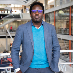
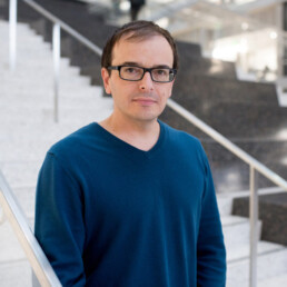
Seth Bank
ECE
Analog/digital alloy semiconductors and metal/semiconductor hetero- and nano-structures
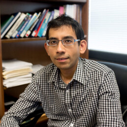
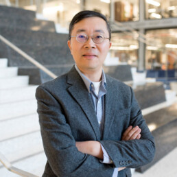
Chih-Hao Chang
ME
Design and fabrication of 2D/3D multifunctional nanostructures with novel physical properties
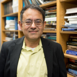
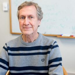
Ananth Dodabalapur
ECE
Nanomanufacturing, two-dimensional material devices, thin-film transistors and circuits
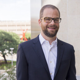
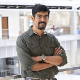
David Pan
ECE
Electronic design automation, manufacturing design, AI-integrated circuit optimization
TIE also plans to work with startups that couldn’t otherwise afford to spin up their own semiconductor manufacturing infrastructure. The organization aims to support a healthy, U.S.-based semiconductor innovation ecosystem.
It can cost hundreds of millions of dollars for semiconductor startups to establish their own infrastructure, which just isn’t feasible,
said S.V. Sreenivasan, professor in the Cockrell School of Engineering’s Walker Department of Mechanical Engineering and TIE’s chief technology officer. We want to derisk hard tech startups and make them more attractive to investors.
TIE was founded three years ago to respond to increased government support for domestic semiconductor manufacturing. Organizers quickly identified packaging, which refers to the variety of shells used to combine and protect the various components, as a vulnerable area. Only 3% of global semiconductor manufacturing work occurs in the U.S., per the U.S. Department of Defense and IPC International, a global electronics association.
After what happened in the pandemic in terms of supply chain issues, it became clear that we needed to focus on improving packaging capacity to ensure that the whole of semiconductor manufacturing processes can be performed domestically,
Sreenivasan said.
The New Frontier: Advanced Packaging
Moore’s Law is an almost 60-year-old observation that the number of transistors that can fit on a chip doubles every two years, bringing massive increases in efficiency with minimal increased costs. This law, most semiconductor experts say, is reaching its maturity. Sustained progress requires new ways to improve chips as demand for improved power and efficiency continues to rise.
The new idea in the field is known as ‘more than Moore,’
said Banerjee, a professor in the Chandra Family Department of Electrical and Computer Engineering who has taught and researched semiconductors for 37 years at UT after working at Texas Instruments for several years. The idea is, we overcome the end of exponential growth of transistors by using new materials and design techniques. That’s the thought behind heterogeneous integration, where we make all kinds of chiplets — electronic chips, optical chips, sensors — stacked on top of one another.
Heterogeneous means something composed of different parts. And heterogeneous integration is part of the larger movement of advanced packaging. Instead of trying to pack single chips with more transistors, this new paradigm uses smaller specialized chips with a single function — the chiplets Banerjee referred to — and packages them together, often in three-dimensional alignments.
It’s actually a lot like LEGOs. Imagine that each different LEGO piece represents a single, smaller chip with its own purpose. The red block controls memory, the blue one represents processing and the yellow one performs communications. With heterogeneous integration, those LEGO blocks can be mixed and matched to make chips for a variety of uses.
Heterogeneous integration is a lot like LEGOs. See for yourself.
These chiplets are less expensive to make, and allow for customized chips to meet specific needs. A huge company isn’t going to make semiconductors specifically to test for a single rare disease, for example, because today that kind of small-batch production is too cumbersome and expensive. But heterogeneous integration can change that.
The next step on the path to these highly specialized chips is combining different materials on a single device.
The next frontier is multi-material, 3D heterogeneous integration where instead of using silicon-only LEGO blocks, so to speak, we bring in many different types of semiconductor materials,
said Sreenivasan. It’s a hard problem with a huge payoff; it’s what we need to address these highly intensive applications.
One of a Kind Program
The massive demand for semiconductors means an already short-staffed industry will need many more workers. According to a 2023 report by the Semiconductor Industry Association, the industry’s workforce will grow by nearly 115,000 jobs by 2030. However, due to national degree completion rates in related disciplines, approximately 67,000 new jobs are at risk of going unfilled — 27,300 of which are for engineers.
This urgent need for talent galvanized the creation of several new educational semiconductor programs at the Cockrell School. Starting this fall, UT will offer a new master’s of semiconductor science engineering degree program.
It stands out as the only in-person master’s degree program at a top-10 nationally ranked engineering school exclusively dedicated to semiconductors. It offers students the opportunity to work in real-world cleanrooms alongside industry partners.
There aren’t many places to get experience with production-level semiconductor equipment at a master’s level,
said Michael Cullinan, associate professor in the Walker Department of Mechanical Engineering and director of the master’s program. And nobody does it in a way that you can do research, work closely with leading companies and learn how the ecosystem actually works.
Sirish Oruganti is a fourth-year Ph.D. student focused on semiconductors.
The program is a collaboration between the Cockrell School and the College of Natural Sciences, and it includes approximately 40 affiliated faculty. The program features aspects of semiconductor manufacturing, device design, circuit and system design, metrology and packaging.
Each job in the industry requires its own set of skills and experience. Companies need engineers to develop new equipment, process engineers to make sure everything is running properly, design engineers to design the chips and work with manufacturing teams to scale them, supply engineers to ensure the right components get to the right places on time, and technicians to run and maintain the equipment.
To build this diverse workforce, UT is creating several other educational offerings. The Texas Engineering Executive Education program offers an online, stackable certificate program for people already in the field who want to level up their skills or to help transition into the field.
Hands-on labs and new educational programs are critical to prepare students for the semiconductor industry.
UT is also partnering with Austin Community College to address every skill set on the semiconductor workforce continuum. Together, they will develop a joint Semiconductor Training Center, allowing students to receive hands-on technical training combined with academic theory. The institutions will also will host programs designed to help people break into the industry advance their careers.
Semiconductor engineering very much falls between multiple disciplines,
Cullinan said. If you do electrical engineering, you’re not getting exposure to manufacturing; if you’re a mechanical engineer you don’t get trained in circuit and device design; and if you’re a chemical engineer you’re not learning about electronics. All of those things are critical components of semiconductor manufacturing, and we have to make sure that our students get an education in all of them.
How We Got Here/What's Next
More than a decade ago, key UT faculty members, including Bonnecaze, Sreenivasan and J. Tinsley Oden, founder of the Oden Institute for Computational Engineering and Sciences, came together to brainstorm ways to use computational technology to create digital twins for microelectronics. They chased a grant program from the National Science Foundation but ultimately didn’t get it.
They went back to the drawing board and decided to broaden their focus and include materials and processes. This time around they got it, and the NAnomanufacturing Systems CENTer (NASCENT) was funded through NSF’s Nanosystems Engineering and Research Center program in 2012. NASCENT is the predecessor to everything that’s happened over the last couple years. TIE is an outgrowth of NASCENT, and many of UT’s semiconductor engineering faculty members, including Cullinan, were hired as part of the center.
NASCENT aimed to build a bridge from science to scalability. It led to the creation of nanomanufacturing systems, nanoscale materials and processes, inline and offline metrology, and functional data analytics for yield management. This infrastructure enabled advances in mobile computing technologies impacting all aspects of health care, education, commerce, communications, computing and lifestyle.
Numerous startups have spun out of NASCENT, including one co-founded by Bonnecaze. Sandbox Semiconductor, led by Bonnecaze’s former student Meghali Chopra, makes computational modeling software for the semiconductor manufacturing industry.
This center helped create connections with industry power players that continue to pay off to this day. Those early connections established relationships that helped the University obtain the DARPA project.
Knowing the current trends in industry — what processes companies invest in, what equipment they’re using — helps faculty members design relevant labs and experiments for students. Among those who have worked in the industry, the students in Banerjee’s course say their lab work translates well to what the big companies are doing.
The fact that they’ve actually made transistors and had a chance to test them and see them operate really helps solidify the theoretical concepts they learn,
Banerjee said. Things don’t always work the way you expect them to work. If you have failed devices, you learn even more because you have to do the detective work to figure out why it didn’t work.
This tight connection with industry has implications for research as well. Texas Engineers have the gaps and challenges first hand and can tune their work to focus on needed advances in materials, packaging, computing and more. Technology created by courageous engineers will have a path to mainstream adoption, pushing the world’s technical capabilities even further.
UT’s prevalence in semiconductors goes beyond the semiconductor space. Having many ways to generate viable prototype electronics quickly could lift UT’s entire research enterprise, specifically for groups that need specialized chips like medicine, aerospace, energy and more.
Traditionally, researchers have to put together a sensor or two by hand in the lab, but a lot of research would benefit from having dozens or hundreds of high quality, customized sensors to take uniform measurements over time,
Cullinan said. Researchers haven’t traditionally had access to that, so there’s opportunity to create chip packages that could, for example, better explore down oil wells or give moon landers more processing capabilities or make medical devices that are more sensitive to enable the use of smaller samples.
WOULD YOU LIKE TO KNOW MORE?
Believe it or not, this is just a snippet of our semiconductor success. The momentum continues to build, see it all as it happens.
